2008 News
Shin-Etsu Chemical has developed a silicone rubber for stamps for micro-contact printing technology
Adaptable for flexible display applications such as active matrix and organic EL displays
Shin-Etsu Chemical Co., Ltd. (President: Chihiro Kanagawa; Head Office: Tokyo), has developed a silicone rubber ideal for a stamp that deposits molecules on surfaces which is essential for micro-contact printing, a key technology of next-generation printable electronics.
Printable electronics is a new component technology that utilizes a printing method that does not require such manufacturing conditions as high vacuum and high temperature that were necessary in existing TFT patterning by photolithography. The applications of this new technology for flexible displays, such as for electronic paper, LCDs and organic electroluminescence (EL) film, are being widely anticipated. Among the printing methods, the micro-contact printing method is the only method that makes it possible to print on a large surface area with hyper-fine submicron meter characteristics, and this method is generating a high level of interest.
This technology is being developed as part of the “Technological Development of Superflexible Display Components” project, commissioned by the New Energy and Industrial Technology Development Organization (NEDO) and is jointly being carried out by the Japan Chemical Innovation Institute (JCII) and the National Institute of Advanced Industrial Science and Technology (AIST). In this project, Shin-Etsu is in charge of the development of a polydimethylsiloxane (PDMS)-type of stamp material.
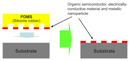
This new silicone rubber product used as the key stamp material for micro-contact printing was developed as a part of this project's research activities. The PDMS stamp, in addition to having the primary function of exactly reproducing and transferring the master mold formed by photolithography, is superior in its suitability as a printing material. Moreover, it also has the characteristic of minimizing the impurities that could become an impediment, and it also features anti-static performance. In the future, this technology is expected to be used in mold material applications in micro-total analysis systems (Micro TAS) and polymer microelectromechanical systems (Polymer MEMS).
Silicones are highly functional materials that combine characteristics of both organic and inorganic materials. They are materials that provide high-value-added features for products in a wide range of industrial fields, including electrical and electronic applications, automobiles, construction, cosmetics and chemicals.
Reference material
Micro-contact printing method using silicone PDMS
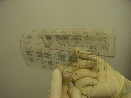
Organic TFT (thin-film transistor) array printed on top of flexible plastic film